Resources
7Semi QFN-32 PCB Adapter Board - Dual-Pitch 0.5mm and 0.65mm SMD-to-DIP Converter for 32-Pin IC Prototyping
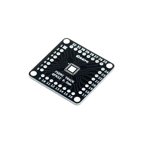
Working with fine-pitch QFN-32 packages during prototyping is one of the most common bottlenecks in embedded development. This adapter board converts compact QFN-32 SMD footprints into a standard 2.54mm DIP format, making them directly compatible with breadboards, development setups, and through-hole prototyping environments. What sets this board apart is its dual-side design - one side accommodates a 0.5mm pitch and the other a 0.65mm pitch - offering support for a broader range of ICs without requiring separate adapters for each variant. The compact 30mm x 30mm form factor, reinforced solder pads, and clearly labelled pin numbering make it well-suited for repeated use across development cycles.
This adapter is particularly useful for engineers and developers working with STM32 microcontrollers, AVR-based devices, ESP32 modules, and a wide range of power management or interface ICs available in QFN-32 packaging. The PCB features clean routing, Pin-1 orientation marking, and a robust 1.7mm board thickness that ensures mechanical stability during soldering and testing. Whether you are running signal validation, peripheral testing, or rapid proof-of-concept builds, this board eliminates the need for custom-designed PCBs and reduces turnaround time significantly. It is equally practical for students, startup teams, and professional electronics engineers looking for a reliable, reusable SMD-to-DIP solution.
Key Features
- Dual-Pitch Support: Accommodates QFN-32 packages with 0.5mm pitch on one side and 0.65mm pitch on the other side, covering 2 of the most widely used QFN-32 footprint variants
- SMD-to-DIP Conversion: Converts QFN-32 SMD packages to a standard 2.54mm DIP format for direct breadboard and through-hole prototyping compatibility
- Compact Form Factor: Measures 30mm x 30mm x 1.7mm, keeping the board small enough for tight prototyping layouts without sacrificing pad accessibility
- Clear Pin Identification: Includes printed pin numbering and a Pin-1 indicator to reduce wiring errors and speed up IC placement
- Reinforced Solder Pads: Robust copper pads provide strong solder joints and reliable electrical connections under repeated use
- Single-Side Operation: Only 1 side of the board should be used at a time; the dual-side layout supports different ICs, not simultaneous use
- Breadboard Compatible: 2.54mm DIP spacing fits standard full-size and half-size breadboards without adapters or modification
- No Custom PCB Required: Eliminates the need to design or fabricate a custom breakout board, saving development time and cost
Applications
- Prototyping STM32, AVR, and ESP32 microcontrollers in QFN-32 packages on breadboards
- Evaluating power management ICs, interface controllers, and RF modules packaged in QFN-32 footprints
- USB-to-serial and I2C/SPI peripheral testing during firmware development
- Academic and laboratory use for embedded systems coursework and electronics experimentation
- Startup and R&D teams building proof-of-concept hardware before committing to full PCB layouts
- Rework and IC validation when a custom breakout board is unavailable or impractical