Resources:
Datasheet
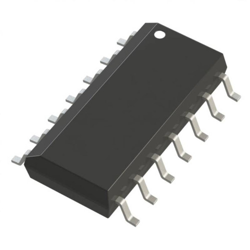
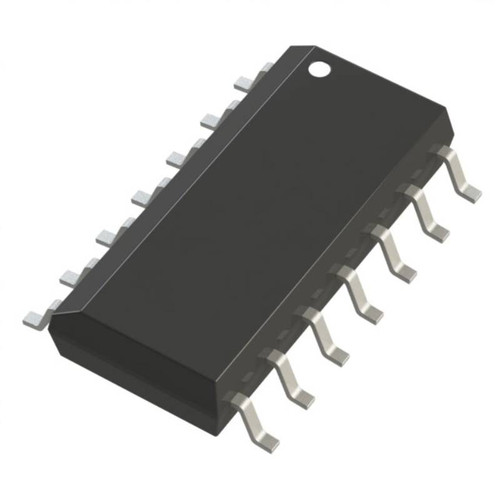
HEF4093BT,653 Quad 2-Input NAND Schmitt Trigger with 3–15 V CMOS Operation and High Noise Immunity
The Nexperia HEF4093BT,653 is a quad 2-input NAND gate IC featuring Schmitt-trigger inputs for reliable processing of slowly changing, noisy, or irregular digital signals. It integrates 4 independent NAND gates, each with 2 Schmitt-trigger inputs that convert gradual input transitions into sharply defined, jitter-free output signals. The device operates across a wide 3–15 V supply range, making it suitable for CMOS logic systems, timing circuits, signal-conditioning applications, waveform generation, and industrial electronics.
The HEF4093B inputs include clamp diodes, allowing current-limiting resistors to be used when interfacing signals that can exceed the supply voltage. Its CMOS architecture provides low power dissipation, high noise immunity, fully static operation, and symmetrical output characteristics. The HEF4093BT,653 is supplied in a compact 14-pin SOIC package and supports operation from -40°C to +125°C, making it suitable for demanding embedded and industrial designs.
Key Features
- Quad NAND Configuration: Integrates 4 independent 2-input NAND gates in a single IC.
- Schmitt-Trigger Inputs: Converts slow or noisy input transitions into clean, sharply defined digital outputs.
- 3–15 V Supply Range: Supports a broad range of CMOS logic and control-system supply voltages.
- 5 V, 10 V and 15 V Ratings: Electrical characteristics are specified at commonly used CMOS supply levels.
- High Noise Immunity: Schmitt-trigger hysteresis improves immunity to noise and unstable input transitions.
- CMOS Low-Power Operation: Suitable for systems requiring low static power consumption.
- Fully Static Operation: Does not require a minimum clock frequency for correct logic operation.
- Input Clamp Diodes: Allow current-limiting resistors to be used when interfacing inputs above VDD.
- Symmetrical Outputs: Standardised output characteristics simplify CMOS logic integration.
- Typical 0.7 V Hysteresis at 5 V: Schmitt-trigger action provides defined switching separation for noisy signals.
- Typical 1.0 V Hysteresis at 10 V: Increased hysteresis supports reliable switching at higher supply levels.
- Typical 1.3 V Hysteresis at 15 V: Provides strong noise discrimination in 15 V CMOS systems.
- 60 ns Maximum Propagation Delay at 15 V: Supports moderate-speed digital and timing applications with 50 pF output loading.
- Low Input Leakage: Input leakage is specified up to ±1 uA at 15 V across the extended temperature range.
- JEDEC JESD 13-B Compliance: Designed according to standardised CMOS logic requirements.
- HBM ESD Protection: Human-body-model protection exceeds 2,000 V.
- CDM ESD Protection: Charged-device-model protection exceeds 1,000 V.
- Wide Temperature Range: Rated for operation from -40°C to +125°C.
- SOIC-14 Package: Compact surface-mount package with 1.27 mm lead pitch.
- Tape-and-Reel Packaging: HEF4093BT,653 is suitable for automated PCB assembly.
Applications
- Wave shaping
- Pulse shaping
- Astable multivibrators
- Monostable multivibrators
- Oscillator circuits
- Timing circuits
- Switch debouncing
- Signal conditioning
- Noise filtering
- Logic-level processing
- Pulse generation
- Sensor signal conditioning
- Industrial control circuits
- Embedded systems
- CMOS logic systems
- Alarm and timing circuits