How MEMS Sensors Actually Work: From Silicon to Smart Devices
Published by Sobhit Chatarjee on 13th Aug 2025
MEMS sensors, smaller than a grain of sand, power most of your smart devices. These technological marvels measure between 1 to 100 micrometers—typical devices range from 20 micrometers to a millimeter.
The term MEMS technology emerged in 1986 and changed how we interact with electronic devices. Your smartphone's orientation and car's airbag system demonstrate MEMS sensor principles. These microsystems convert mechanical, magnetic, or chemical changes into electrical information with precision. They achieve resolutions of 0.0001° and operate in extreme temperatures from -40°C to +85°C.
MEMS sensors' importance shows in their market growth from $40 billion in 2006 to $72 billion by 2011. Bosch alone produces more than four million MEMS sensors daily for mobility solutions and consumer electronics. These sensors excel in automotive airbag systems, inkjet printers, and medical devices. Their budget-friendly design combines high accuracy with low power consumption, high sensitivity, and durability.
This piece explains MEMS sensors' core concepts, operational principles, available types, manufacturing processes, and applications that shape industries worldwide.
Table of Contents:
- What is a MEMS Sensor and Why It Matters
- Understanding the MEMS Sensor Working Principle
- Types of MEMS Sensors and Their Functions
- From Silicon to Sensor: MEMS Fabrication Process
- Applications of MEMS Sensors Across Industries
- Conclusion
- FAQs
What is a MEMS Sensor and Why It Matters
MEMS sensors stand out as one of the biggest breakthroughs in modern electronics miniaturization. Micro-Electro-Mechanical Systems (MEMS) are tiny integrated devices that blend mechanical structures with electrical circuits to detect and measure physical phenomena. These amazing sensors have reshaped the scene in countless industries by providing accurate measurements in incredibly small packages.
Definition of MEMS: Micro-Electro-Mechanical Systems
MEMS sensors are tiny devices that turn physical phenomena from nature into electrical signals. The name "Micro-Electro-Mechanical Systems" tells us exactly what these sensors are—microscopic systems that combine electrical and mechanical parts to do specific jobs. Each device has a central unit that processes data (usually an integrated circuit chip like a microprocessor) and several parts that work with the environment, such as microsensors.
MEMS sensors beat conventional electromechanical systems in three main ways:
-
Space-efficient designs through miniaturization
-
Sensors and electronics combined on one device
-
Low-cost mass production capabilities
These sensors work as transducers that turn mechanical signals into electrical or optical ones. This makes them vital parts in countless applications where electronic systems need to process physical measurements.
Scale and Structure: 1-100 Micrometer Components
MEMS components usually measure between 1 and 100 micrometers (0.001 to 0.1 mm). Complete MEMS devices range from 20 micrometers to a millimeter. A human hair is many times bigger than these tiny components.
Physics works differently at this microscopic scale compared to larger mechanical devices. MEMS's large surface area to volume ratio means that ambient electromagnetic forces (like electrostatic charges and magnetic moments) and fluid dynamics (including surface tension and viscosity) become crucial design factors. As size gets smaller, component masses and inertias decrease faster, while surface and tribological effects matter more.
Integration of Mechanical and Electronic Elements
MEMS technology's real breakthrough comes from putting mechanical structures and electronic circuits together on one substrate. Manufacturers use many of the same batch fabrication techniques as the integrated circuit industry. This shared approach lets them create mechanical and electronic components at the same time, which results in highly integrated systems.
Every MEMS sensor combines multiple working elements. The mechanical parts might have structures like diaphragms, beams, levers, springs, and even tiny gears etched or deposited onto silicon substrates. The electronic components handle data sensing and processing.
These sensors use a 3D architecture where actuators do mechanical operations and sensors create electrical signals when forces hit their elements. This three-dimensional design uses silicon's unique mechanical properties to sense acceleration, rotation, angular rate, vibration, and many more physical and environmental properties.
MEMS technology shows great promise for future state-of-the-art developments by combining microsensors, microactuators, and microelectronics on a single microchip. This combination creates complete "systems" instead of just devices, where mechanical and electrical parts work together to perform complex tasks.
Understanding the MEMS Sensor Working Principle
MEMS sensors work by detecting tiny physical changes and turning them into measurable electrical signals. These microscopic sensors employ fundamental physical properties that give them amazing sensitivity in a tiny package. The elegant engineering behind these small devices powers many modern technologies we use today.
Capacitive Sensing Mechanism in MEMS
Capacitive sensing serves as the main detection method in most MEMS sensors. The system measures capacitance changes between two or more electrodes when physical parameters change. A simple MEMS capacitive sensor has parallel conductive plates with a small gap between them. The capacitance changes when these plates move relative to each other.
The science behind this follows a simple parallel plate capacitor equation: C = (ε₀εᵣA)/d, where C represents capacitance, ε₀ is the permittivity of free space, εᵣ is the relative permittivity of the dielectric medium, A is the effective surface area, and d is the separation distance between plates. Even the smallest changes in this distance create measurable variations in capacitance.
Capacitive sensing beats other methods in several ways. To cite an instance, see optical sensing - while it works well, it costs too much to set up. Capacitive techniques give excellent resolution more economically. On top of that, it shows better stability across temperature ranges with a temperature coefficient parameter of just 0.03%, nowhere near the 0.27% seen in piezoresistive alternatives.
Role of Suspended Mass and Electric Potential
A suspended mass sits between capacitive plates at the core of many MEMS sensors. This mechanical structure helps the sensor detect environmental changes. The suspended mass changes position from its resting state when external forces like acceleration or tilt affect the sensor.
This movement creates vital changes in electric potential between the mass and fixed capacitive plates. The capacitance distribution changes as the suspended mass moves closer to one plate and away from another. These systems achieve remarkable sensitivity - high-precision MEMS inclinometers can detect movements as small as 0.0001° despite their microscopic size.
Different sensor types have unique movement mechanisms. The flexible diaphragm in pressure sensors changes shape with pressure, which changes the gap between electrodes. Accelerometers use structures that look like tiny hair brushes with interdigitated fingers that move when acceleration forces act on them. Each design tweaks the suspended mass setup to measure specific things better.
Signal Conversion: Capacitance to Electrical Output
Complex processing circuits turn tiny capacitance changes into useful electrical signals. Special transimpedance amplifiers or capacitance-to-voltage converters boost these small variations first. These circuits can detect capacitance differences that measure just fractions of a femtofarad (10^-15 farads).
The conversion happens in several steps:
-
Capacitance variations create voltage or current changes
-
Filters remove noise and isolate the measurement
-
More amplification prepares the signal for output
-
Final conversion creates stable outputs as digital signals, 4-20mA current loops, or voltage signals
MEMS sensors often use differential sensing setups to boost accuracy. Reference capacitors stay stable during environmental changes, letting the system measure relative differences instead of absolute values. This method reduces signal drift from temperature changes and manufacturing variations effectively.
Signal conversion faces a big challenge from parasitic capacitance, which can match the sensor capacitance in size. Special readout circuits solve this using techniques like correlated double sampling, negative capacitance compensation, and switched-capacitor schemes that separate the real signal from parasitic effects.
Types of MEMS Sensors and Their Functions
MEMS sensors are available in many specialized forms. Each sensor measures specific physical phenomena with remarkable precision. These microscopic devices employ different detection mechanisms that serve applications in many industries, from consumer electronics to automotive safety systems.
MEMS Accelerometers for Motion Detection
MEMS accelerometers detect and measure acceleration, tilt, shock, and vibration in performance-driven applications. These sensors employ capacitive detection principles where a suspended mass changes position under acceleration forces. Most accelerometers provide measurement ranges from ±2g to ±16g with 12-bit resolution and excellent sensitivity for motion detection. These devices fall into two categories: variable capacitive (highly sensitive) and piezoresistive (low-range) types. Today's accelerometers offer advanced features like activity/inactivity monitoring, free-fall detection, and work well in temperatures from -40°C to +125°C. You'll find them in automotive safety systems (airbags, stability control), consumer electronics (smartphones, gaming controllers), industrial monitoring, and healthcare devices.
MEMS Gyroscopes for Angular Velocity
MEMS gyroscopes measure angular velocity—the speed of rotation around an axis in degrees per second (°/s) or revolutions per second (RPS). Unlike traditional gyroscopes, MEMS versions use vibrating structures instead of rotating components. These devices work on the Coriolis effect principle, where a vibrating proof mass experiences force perpendicular to its motion direction and rotation axis. The resulting displacement shows up as changes in capacitance. MEMS gyroscopes measure three components of angular motion: roll, pitch, and yaw. Navigation systems, drones, virtual reality devices, and automotive stability control systems commonly use these sensors.
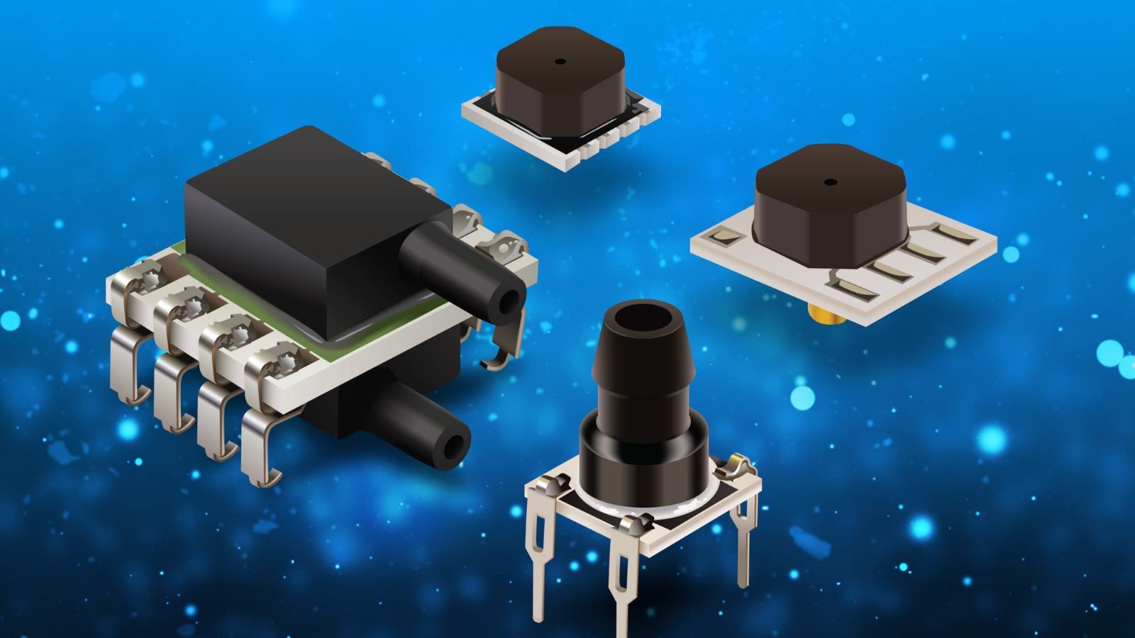
MEMS Pressure Sensors for Fluid Systems
MEMS pressure sensors use piezoresistive pressure sensing dies processed through MEMS technology. A springy diaphragm with integrated resistors forms the core component, creating a Wheatstone bridge structure. Pressure deforms this diaphragm, which changes the resistance proportionally and creates a measurable electrical signal. These sensors measure absolute pressure ranges from 260 to 1260 hPa or up to 4060 hPa. You can find them as absolute, vacuum, sealed, gage, and differential pressure sensors. Automotive systems (tire pressure monitoring), medical devices (blood pressure monitoring), industrial automation, and environmental monitoring all benefit from these sensors.
MEMS Microphones and Environmental Sensors
MEMS microphones work as electro-acoustic transducers that combine a sensor and application-specific integrated circuit in one package. These devices turn sound pressure variations into capacitance changes that become electrical signals. Their high acoustic overload points (AOP) and excellent signal-to-noise ratios (SNR) make them perfect for applications needing wide dynamic range. MEMS environmental sensors also detect various gasses, monitor airflow, and measure other environmental parameters. Smartphones, wearables, automotive systems, smart homes, and industrial monitoring equipment all use these sensor types.
From Silicon to Sensor: MEMS Fabrication Process
Raw silicon transforms into sophisticated MEMS sensors through precise microfabrication processes. These manufacturing techniques blend traditional integrated circuit methods with specialized micromachining steps. This combination creates three-dimensional mechanical structures at microscopic scales.
Photolithography and Patterning Techniques
Photolithography defines patterns in MEMS fabrication. The process moves patterns to photosensitive materials (photoresists) by exposing them to light sources. Specific wavelengths change the chemical resistance of photoresist to developer solutions. Positive photoresists dissolve in exposed regions. Negative photoresists become resistant to developers after exposure. These patterns work as temporary masks for etching underlying layers or templates for material deposition. Complex structures need precise alignment marks between different layers. These marks ensure accurate registration.
Wet vs Dry Etching in MEMS Manufacturing
Etching processes carve out intricate structures vital to MEMS functionality. Wet etching uses chemical solutions (acids, bases, solvents) to remove material and offers high selectivity and etch rates. The process creates isotropic profiles that etch uniformly in all directions. Dry etching uses plasma or ionized gasses and creates better anisotropic profiles with vertical sidewalls. This makes it perfect for high-aspect-ratio structures and precise features. Engineers choose between these methods based on profile control needs, surface quality requirements, and material compatibility.
Material Choices: Silicon, Polymers, Metals, Ceramics
Silicon dominates MEMS manufacturing because it's cheap, readily available, and has exceptional mechanical properties. Its perfect elasticity allows billions of movements without breaking. Polymers like SU-8 and polydimethylsiloxane work better for biomedical MEMS. These materials offer simpler manufacturing and play well with living tissues. Gold, aluminum, and copper make excellent electrodes, interconnects, and sensing elements. Their conductivity and elastic properties shine in these roles. Material choice shapes performance, reliability, and manufacturing costs.
Wafer Bonding and Packaging Methods
Wafer bonding creates complex 3D structures by joining multiple wafers or sealing them hermetically. Direct (fusion) bonding joins silicon wafers through high-temperature annealing. Anodic bonding connects silicon to glass with electric fields at high temperatures. Eutectic bonding uses metal layers with different melting points (usually Au-Sn or Au-In systems) to create strong joints at lower temperatures. The packaging process protects MEMS devices and keeps them stable. Methods range from metal can packages to ceramic window packages. Packaging takes up 50-90% of total MEMS fabrication costs.

Applications of MEMS Sensors Across Industries
MEMS sensors are becoming popular in many industries because of their accuracy and small size. These tiny technological marvels now play a key role in everything from safety systems to everyday devices.
Automotive: Airbags, Stability Control, Tire Pressure
MEMS sensors make cars safer in several ways. Their accelerometers detect sudden stops and deploy airbags in milliseconds. Side-impact sensors measure quick pressure changes inside door spaces. The car's stability control system uses MEMS gyroscopes and accelerometers to keep control during skids. These sensors compare the car's speed, motion, and steering angle. MEMS-based tire pressure systems warn drivers about dangerous pressure drops, which helps with safety and saves fuel. These sensors also work in electric vehicles, where they check battery conditions to stop thermal problems in lithium-ion batteries.
Consumer Electronics: Smartphones, VR, Wearables
MEMS sensors make our electronic devices work better and easier to use. Today's smartphones have several MEMS sensors. Accelerometers help rotate screens and recognize gestures, while gyroscopes and magnetometers provide motion sensing for navigation and AR apps. VR systems need MEMS gyroscopes to track head movements accurately. Health trackers use MEMS accelerometers and pressure sensors to check activities and surroundings. Market data shows that wearable devices in 2019 had 4.1 sensor elements on average, up from 1.4 in 2013.
Medical Devices: Lab-on-a-Chip, Pressure Monitoring
The medical industry has welcomed MEMS technology for its precision and small size. MEMS biosensors detect biological samples quickly without labels, which helps catch diseases early. MEMS pressure sensors track vital signs during surgery, including blood pressure. Some of these devices are tiny - just 1mm × 0.7mm × 0.175mm - small enough to fit in catheters. Organ-on-a-chip systems copy human organs in basic form and mimic the body's physical conditions.
Industrial Automation and Smart Manufacturing
MEMS sensors make factories work better and safer. Flow sensors watch air movement to keep dust away from production lines. Robot fingertips with MEMS 6-axis force torque sensors can now handle soft objects that only humans could manage before. MEMS accelerometers and temperature sensors spot machine problems before they break down. This cuts costs and makes equipment last longer.
Conclusion
MEMS sensors have without doubt changed modern technology with their remarkable blend of microscopic size and exceptional precision. You've learned how these tiny devices—often smaller than a grain of sand—convert physical phenomena into electrical signals through sophisticated sensing mechanisms. These miniature marvels combine mechanical structures with integrated electronics on a single silicon substrate. This combination enables unmatched functionality in devices you use daily.
On top of that, different types of MEMS sensors serve specialized functions in many applications. Your smartphone's accelerometers detect motion and orientation changes, while gyroscopes measure angular velocity for navigation systems and virtual reality headsets. Pressure sensors monitor everything from tire pressure to blood pressure. Microphones and environmental sensors make interaction with smart devices better. Each type shows MEMS technology's versatility through different sensing principles adapted to specific measurement needs.
Making these sophisticated sensors needs precise microfabrication techniques. Photolithography creates intricate patterns, and specialized etching processes carve three-dimensional mechanical structures from silicon wafers. Material choice—whether silicon, polymers, metals, or ceramics—affects performance characteristics and application suitability. The progress of these manufacturing processes has led to MEMS technology's widespread adoption across industries.
MEMS sensors keep improving innovation in countless fields. These microscopic systems are the foundations of technologies that improve safety, efficiency, and user experience—from life-saving automotive applications to innovative medical devices. Manufacturing techniques will advance further, and MEMS sensors will definitely become smaller, more energy-efficient, and more capable. This progress will enable the next generation of smart devices and systems that will change how you interact with technology.
FAQs
Q. How do MEMS sensors function in smart devices?
A. MEMS sensors convert physical or environmental stimuli into electrical signals. They use tiny mechanical structures and electrical circuits integrated on a single chip to detect changes in motion, orientation, pressure, and other parameters. This allows smart devices to respond to their environment and user interactions.
Q. What are the common types of MEMS sensors found in smartphones?
A. Smartphones typically incorporate several MEMS sensors, including accelerometers for detecting motion and orientation, gyroscopes for measuring angular velocity, and magnetometers for sensing magnetic fields. These sensors enable features like screen rotation, navigation, and augmented reality applications.
Q. How accurate are MEMS sensors?
A. MEMS sensors can be highly accurate despite their small size. For example, some MEMS inclinometers can detect movements as small as 0.0001°. However, the accuracy can vary depending on the specific type and application of the sensor.
Q. What is the manufacturing process for MEMS sensors?
A. MEMS sensors are manufactured using microfabrication techniques similar to those used in integrated circuit production. The process involves photolithography for pattern creation, etching to remove material, and the deposition of various materials like silicon, polymers, and metals. Wafer bonding and specialized packaging methods are also crucial steps in the fabrication process.
Q. In which industries are MEMS sensors commonly used?
A. MEMS sensors find applications across numerous industries. They are widely used in automotive safety systems (airbags, stability control), consumer electronics (smartphones, wearables), medical devices (pressure monitoring, lab-on-a-chip), and industrial automation (predictive maintenance, robotics). Their small size, low cost, and high accuracy make them valuable in many technological applications.